Watch the Video:
Using ROMs as Combinational Logic (Opens in New Tab)
(Page restored from wayback machine)
During my teen years I read a book about the Z80 processor that had a few paragraphs in the back that described using an EPROM as a 7 segment display decoder in order to have custom display patterns. Recently during my Z80 project I remembered this information while I was considering address decoding and programmable logic.
Watch the Video:
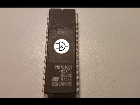
This method can be achieved with a standard ROM's* and a compatible programmer. For this paper I will be using a M27C256B a 32Kbyte EPROM from Stmicro as my example. The principles used for this EPROM should be identical to other ROM's available, as long as they can be directly addressed and give a direct data output then it should work.
*EPROM, PROM, ROM, FlashROM (All must be the parallel variety)
This EPROM has 15 address lines and 8 data lines, when we use EPROM's as combination logic, we use the address lines as inputs and the data lines as outputs. Most EPROM's run at TTL level so it will be perfect for decoding logic in a computer circuit. The speed of EPROM's vary depending on the manufacturer and model number, this you would have to check in the datasheet for the device you plan to use, usually older the device the slower it is. A modern FlashROM would generally be faster than the older EPROM but you would have to be careful about mixing TTL and LVTTL standards, this is something you would have to check with in the device's datasheet.
In order to use this as combination logic we first need to decide what we will be doing with each output line (data lines). We start by determining how many outputs are going to be needed, then we create a Boolean equation for each output line using the address lines as inputs. We then translate the Boolean equations into a truth tables, combine these truth tables into a single binary mapping which will then be programmed into the ROM. Keep in mind that the number of outputs you use will not increase the complexity and size of the binary mappings, but for every extra input (address line) you use, you double the size of the binary mapping.
Let's do an example using a single gate, with 2 inputs and 1 output. We will make an AND gate.
Inputs: A0, A1 | Outputs: D0
Equation: D0 = A0 * A1
| A1 | A0 | D0 |
|---|---|---|
| 0 | 0 | 0 |
| 0 | 1 | 0 |
| 1 | 0 | 0 |
| 1 | 1 | 1 |
Converting the truth table to a binary mapping is simply finding where the address of the mapping has the same matching configuration as the address lines used for input, then taking the output bit and using setting the same bit on the data line of the mapping. Due to the frequency the lower address lines change at, the equations that use those lines will be duplicated many times.
| Address | Data |
|---|---|
| 000 0000 0000 00 00 | 0000 000 0 |
| 000 0000 0000 00 01 | 0000 000 0 |
| 000 0000 0000 00 10 | 0000 000 0 |
| 000 0000 0000 00 11 | 0000 000 1 |
| 000 0000 0000 01 00 | 0000 000 0 |
| 000 0000 0000 01 01 | 0000 000 0 |
| 000 0000 0000 01 10 | 0000 000 0 |
| 000 0000 0000 01 11 | 0000 000 1 |
| 000 0000 0000 10 00 | 0000 000 0 |
| 000 0000 0000 11 01 | 0000 000 0 |
If you are only using a few inputs, then you can ground the unused inputs and not have to repeat the pattern throughout the entire address range, this is helpful if you are translating this by hand.
Building on the first example, we will add an OR gate into the device.
Inputs: A2, A3 | Outputs: D1
Equation: D1 = A2 + A3
| A3 | A2 | D1 |
|---|---|---|
| 0 | 0 | 0 |
| 0 | 1 | 1 |
| 1 | 0 | 1 |
| 1 | 1 | 1 |
The truth table above will translate to the following adding on to what has already been used.
| Address | Data |
|---|---|
| 000 0000 0000 0000 | 0000 00 00 |
| 000 0000 0000 0001 | 0000 00 00 |
| 000 0000 0000 0010 | 0000 00 00 |
| 000 0000 0000 0011 | 0000 00 01 |
| 000 0000 0000 0100 | 0000 00 10 |
| 000 0000 0000 0101 | 0000 00 10 |
| 000 0000 0000 0110 | 0000 00 10 |
| 000 0000 0000 0111 | 0000 00 11 |
| 000 0000 0000 1000 | 0000 00 10 |
| 000 0000 0000 1001 | 0000 00 10 |
| 000 0000 0000 1010 | 0000 00 10 |
| 000 0000 0000 1011 | 0000 00 11 |
| 000 0000 0000 1100 | 0000 00 10 |
| 000 0000 0000 1101 | 0000 00 10 |
| 000 0000 0000 1110 | 0000 00 10 |
| 000 0000 0000 1111 | 0000 00 11 |
You can see from the mapping that the data from the truth table translates easily. You keep building up the mapping in this fashion until you have accounted for all inputs and outputs that are being used. This method isn't limited to 2 input gates, or even to just single gates themselves, you can convert an entire circuit into this form as long as it's combination.